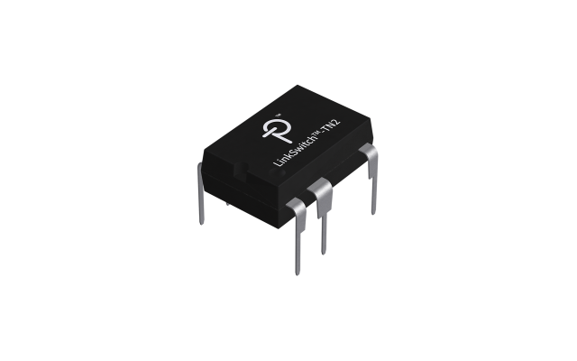
Product details
LinkSwitch - TN2 series IC is suitable for the isolated an off-line power supply, and compared the traditional linear or resistance capacity step-down scheme has improved performance.The high integration of LinkSwitch - TN2 IC design has more applicability, and with higher efficiency, more comprehensive system level protection and higher reliability.The product series support step-down, buck - boost and flyback converter topology.Each device on a single chip IC used a 725 V / 900 V power MOSFET, oscillator, which can realize the highest light load efficiency of on/off control, one for IC implementation from the power supply of high voltage switch the current source, frequency modulation, fast cycle (by) current limit, hysteresis heat shut off and the output and input over-voltage protection circuit.
LinkSwitch - TN2 IC current consumption in standby mode, so that the power supply design in the no-load and standby power consumption of the global all standard.LinkSwitch - TN2 device also has a higher precision reference voltage feedback pin, plus or minus 1.3%, the previous generation devices (LinkSwitch - TN) reference voltage accuracy of 6.6%.MOSFET work current limit point can be through the BYPASS pin capacitance value choice.Choose high current limit point can provide maximum continuous output current, and low current limit points allows the use of very low cost small size surface-mount inductor.Perfect protection feature to ensure power supply safe and reliable operation, in case of input and output overvoltage fault, overheating fault device, voltage imbalance, and the power supply output overload or short circuit fault protection devices and the whole system.
The product features
Performance characteristics and design suitability
- Support the step-down type, buck - boost type and flyback topology
- Very small element step-down converter
- Good load regulation and the input voltage regulation
- The optional components to current limit point
- Working frequency of 66 kHz, and has accurate current limit point
- Allows the use of commercially available off-the-shelf inductance low cost
- Can reduce the size of the inductance and capacitance and cost
- The frequency modulation technology can reduce the complexity of the EMI filter circuit
- Pin layout conducive to heat dissipation on the PCB design
Enhanced safety and reliable performance
- Output overvoltage protection (OVP)
- Input overvoltage protection (ovf)
- Hysteresis overheating protection (OTP)
- Expanded the drain and the creepage distance between other pins, improve the reliability of the application
- Integration of 725 V rated voltage MOSFET, have excellent resistance to lightning performance
- 900 V MOSFET series is suitable for the industrial application or provide greater safety margin
EcoSmart, high efficiency and energy saving
- Standby power supply IC when current < 100 mu A
- On/off control can provide constant efficiency in a wide load range
- Easily meet all energy efficiency standards around the world
- Using external offset when the power supply of high-end step-down converter topology of no-load power consumption < 30 mW
- The flyback converter using external bias power supply when the topology of the no-load power consumption < 10 mW
Product specification
| Output current (maximum) - CCM, 230 v | 775 mA |
| Output current (maximum) - MDCM, 230 v | 485 mA |
| Output current (maximum) - MDCM, general | 485.00 mA |
| Output current (maximum) - CCM, general | 775.00 mA |
| The breakdown voltage | 725 V |
| The input voltage (minimum) | 85 V |
| The input voltage. | 265 V |
| Automatic restart and overpressure reactions | Auto - restart |
| IC packaging | PDIP - 8 c |
| Internal switch | Yes |
| Installation type | Through Hole, |
| Overheating reaction | Hysteretic |
| Operating temperature (minimum) | To 40 ° C |
| Operating temperature (maximum) | 150 ° c. |
| The control mode | Primary side - |
| Control function |
Selectable Current Limit
Frequency Jittering
Soft Start
On/Off Control |
| Protection function |
Input Overvoltage
The Output Open Loop
The Output Overload
The Output Overvoltage
The Output Short Circuit
Overtemperature |
| Output configuration | CV |
| topology |
Buck - Boost
Flyback |
| The Product Sub - Type | PMIC |
| Secondary response | Auto - restart |


